The function of the on-board electronic compass is to help the user to determine the driving direction of the vehicle, accurately display the azimuth angle and provide correct operation instructions. Therefore, the accuracy of the navigation becomes an important indicator to measure the performance of the system.
The electronic compass based on the AMR magnetoresistive sensor and the accelerometer ADXL202 introduced in this paper is one of the strapdown inertial navigation systems. In the electronic compass system, the microcontroller VRS51L3074 completes counting the pulse width and period of the output signal of the acceleration sensor, obtains the instantaneous acceleration value of the vehicle, and then uses the trigonometric function relationship to calculate the roll and pitch angles between the current position and the known reference position. , Perform attitude calculations to get the vehicle's heading and azimuth. However, the electromagnetic environment of the automobile is complex, especially the vibration and instantaneous power variation of the automobile will generate spike interference to the duty cycle signal output from the ADXL202, which will seriously affect the accuracy of the counting. Therefore, suppressing the pulse interference is particularly important in improving the counting accuracy and enhancing the system performance.
1ADXL202 working principle ADXL202 sensor is composed of oscillator, X, Y direction sensor, phase detection circuit and duty cycle modulator, with digital output interface and analog voltage signal output interface. The X and Y direction sensors are two orthogonal acceleration sensors. When the ADXL202 changes with respect to the ground plane direction, the X and Y directions correspond to different outputs, so that the dynamically changing acceleration and the constant acceleration can be measured. The sensor's post-stage phase detector is mainly used to correct the signal and determine the direction of the signal. The output from the detector is driven by a 32kΩ resistor to drive the duty cycle modulator. The bandwidth can be changed by designing the external capacitors CX and CY on the XFILT and YFILT pins. At the same time, external capacitors have a certain effect on filtering noise and suppressing zero drift.
After the signal passes through the low-pass filter, the duty cycle modulator converts the signal to a digital signal output. Through the external resistance of T2 pin can change T2 cycle T2 (1 ~ 10ms), which is convenient to use in different occasions with different precision requirements. The output duty signal can be calculated by the counter duty cycle. The acceleration can be calculated by formula (1).
When the acceleration is 0g, the duty ratio of the output signal is 50%; the duty ratio of the pulse width caused by the sensitivity per 1g changes by 12.5%. The offset and system error at 0g in the application affect the actual output value. The inclination of the X and Y axes can be calculated based on the measured acceleration values:

When the accelerometer is oriented, its X and Y axes are parallel to the Earth's surface and can be used as a dual axis tilt sensor with both roll and tilt axes. The pitch angle of the measured object is denoted by γ and the roll angle β. The three sensitive axes of the magnetoresistive sensor are installed along the three coordinate axes of the carrier, and the projection components (HX, HY, HZ) of the magnetic field magnetic field intensity H in three coordinates of the carrier coordinate system are respectively measured, and then the pitch angle and the horizontal direction are used. The attitude of the electronic compass can be obtained by performing the attitude calculation with the roll angle.
2 ADXL202 anti-jamming design idea According to ADXL202 user manual, the sensor and the microprocessor share the power supply will cause interference, so the circuit design uses a solution to suppress interference. The design uses a 0.1μF capacitor and a resistor less than or equal to 100Ω to suppress interference. Experimental tests show that there are still other parts of the circuit where power and sensor power affect each other, and the interference suppression effect is not ideal. After repeated trials, the sensor uses an independent power supply, and the resistance and capacitance of the device and the conditioning signal are placed on a separate board or surrounded by a rough ground wire in an area of ​​the circuit board during the experiment. Room conditions get better interference suppression. However, in actual applications, the vibration and instantaneous power variation of the vehicle will produce spike interference (pulse width of approximately 1 to 2 ms) on the duty cycle signal output from the ADXL202E and cannot be eliminated. This requires more processing. There are many measures to suppress and eliminate the influence of spike interference. Commonly there are hardware methods and software methods, or a combination of both. Considering that the overall volume of the electronic compass and the signal of the magnetoresistive sensor are more sensitive to interference, if an efficient hardware filter is used, the system circuit will become very large; using a simple hardware circuit, the filtering effect is not complete. In fact, it is also possible to eliminate the spike interference by software filtering by means of a microprocessor. The adoption of software filtering algorithm will undoubtedly make the hardware resources of the system more fully utilized while simplifying the circuit structure, and achieve the requirement of reducing the product design cost.
ADXL202E output signal duty cycle adjustment (DCM) cycle is determined by the external resistance, generally lower than 1kHz, so the count input high and low duration of up to several ms or even tens of ms, visible sensor output normal count signal high, low The level change is slower; while the controller pulse width count time is less than 1 μs, the interference spike is abrupt, so the interference can be discerned from the normal count. Therefore, it is feasible to use software filtering to eliminate spike interference.
The VRS51L3074 microcontroller is a member of the 8-bit microcontroller family VRS51L3XXX series introduced by Ramtron of the United States. VRSS1L3074 provides two separate pulse width counter (PWC) modules associated with timers 0 and 1. Users can flexibly control the timer start or stop counting through the configuration of the PWC module and timer, so that they can be conveniently implemented. The pulse width and cycle count of the ADXL202E output.
Count inputs from the microcontroller and observe the signal waveforms. For ease of analysis, several interference spikes are set in the high and low sections, which are labeled as SectionA and SectionC. The falling edge and rising edge of the duty cycle signal are labeled as SectionB and SectionD, respectively. The microcontroller is periodically sampled by the count clock. The "1" in the sampling value indicates that it is high level and the "0" indicates low level. The I/O port samples the status of the duty cycle signal output port and uses a 1-byte variable R to dynamically store the sampled value. For each sampling of the controller, the data in the variable R shifts one bit to the left, the state of the original highest bit of R is removed, and the new sampling state at the current moment is saved to the lowest bit of R, and the variable R is updated. The state memory R holds the sampled values ​​of the most recent 8 sampling cycles.
In FIG. 1, from the normal falling edge process (Section B), it can be seen that the data in the variable R has undergone a process of coexistence from all bits 1 to 1, 0, and then changed to all 0; however, at high power In section A (Section A), the variable R has undergone a process of changing from all 1, to 1, 0, and back to all 1. Similarly, the normal Section_D variable R undergoes a state change process in which all bits are all 0, coexist to 0, 1 and then change to all 1; in the section (SectionC) of the low-level section, the variable R goes through The sampling state is from 0 to 0, 1 mixed, and back to all 0. By judging the different changes of the data in the variable R under these four conditions, the purpose of distinguishing the interference from the normal change can be achieved. This is the basic idea of ​​the software filtering anti-jamming method used in this design.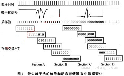 3. Implementation of software filtering algorithm 3.1 Software filtering analysis According to the software filtering design idea, the filtering subroutine is changed by the main program in the signal state and is called when it enters the interrupt. Figure 2 shows the flow of the filtering procedure. The flow chart is analyzed with reference to the four Sections in FIG. When an edge or interference signal (signal cycle is greater than the count clock cycle) arrives, the VPS51L3074 microcontroller PWC count stop condition is met and the system enters the interrupt service routine. In the interrupt subroutine, first reset the pulse width count condition, then sample the current state, sample once, shift the status register to the left by 1 bit, sample it to the high level as “1â€, and sample the low level as "0". If the normal falling edge SectionB, front in the high section, the initial state variable Flag is all 1, when there is a low level, the controller enters the interrupt, followed by 16 samples. It has been mentioned that the peak interference of the system processing is about 1 ~ 2ms, each sample period is about 0.4ms, and the peak interference pulse width is less than 8 sampling periods. The system is designed to sample 16 times. Only the last 8 storage states are compared with the original state. If the last sampling state is “0â€, it is the opposite of the original state, and it can be judged as a normal falling edge. If the interference signal causes count interruption, the first 8 sampling states are not all "1", and the latter 8 states are all "1". The last sampling state is the same as the original state, and it can be judged that this is an interference signal, such as SectionA. During the signal state sampling, the counting condition continues to count until the PWC continues until the actual falling edge arrives, the count stops and is saved, and the counting register is restored to the initial value, so that the interference signal is filtered out. Similarly, the normal rising edge SectionD, the memory original state is "0", the memory state is "1" after the rising edge comes, opposite to the original state, the PWC count stops and saves, the counting register restores to the initial value, exits cuts off the subroutine. After the appearance of the interference signal, the sampling state is the same as the original state, and the interference spike can be filtered out. If you want to make the pulse width count more accurate, you can determine the period of the system's abnormal count in the first 8 sampling cycles and add it to the final count cycle. At this point, the program flow reflects the software filtering function.
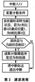
3.2 source code analysis corresponds to the program flow chart, given the microcontroller through the P4.2 port ADXL202 a sampling of the output filter and complete the pulse width of the source code. The source program is as follows: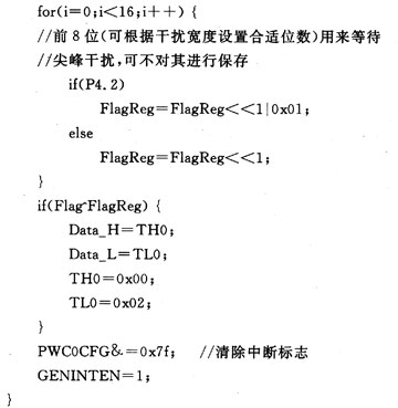
There are three variables defined in the source program, in which the Flag stores the original state value; FlagReg stores the current sample value; the variable i records the number of samples; changing the value of i can control the waiting time for filtering the spike. The program judges whether the current signal is a valid signal or an interfering signal by using the value after the original state and the current sampled state is XORed, so that the intermediate overshoot or spike interference of the rising edge and falling edge is processed correspondingly, and the interruption subroutine is exited. The purpose of counting normal signals and filtering out spike interference is achieved.
4 Test results Because of the conditional restrictions and the randomness of the interference, the test performed on a vehicle-mounted Tunzi compass based on the ADXL202 cannot accurately calibrate the measured angle and the direction angle. During the experiment, the corresponding algorithm was evaluated by the standard deviation of multiple measurements of the same physical quantity under the same conditions. The test results are listed in Table 1. It can be seen from the standard deviation of the experimental test that the software filtering is much smaller, and this software filtering algorithm is very effective in filtering out the spike interference.
Conclusion The software filtering algorithm proposed in this paper is fast, high in code efficiency and ideal in filtering. It is a practical digital filtering design method, which embodies the idea of ​​combining the algorithm with specific hardware. On the other hand, memory variables can be appropriately expanded to multi-byte variables when the pulse disturbance is wide. This algorithm can also be combined with the FPGA for other applications that require high counting accuracy and are susceptible to spike interference.
The electronic compass based on the AMR magnetoresistive sensor and the accelerometer ADXL202 introduced in this paper is one of the strapdown inertial navigation systems. In the electronic compass system, the microcontroller VRS51L3074 completes counting the pulse width and period of the output signal of the acceleration sensor, obtains the instantaneous acceleration value of the vehicle, and then uses the trigonometric function relationship to calculate the roll and pitch angles between the current position and the known reference position. , Perform attitude calculations to get the vehicle's heading and azimuth. However, the electromagnetic environment of the automobile is complex, especially the vibration and instantaneous power variation of the automobile will generate spike interference to the duty cycle signal output from the ADXL202, which will seriously affect the accuracy of the counting. Therefore, suppressing the pulse interference is particularly important in improving the counting accuracy and enhancing the system performance.
1ADXL202 working principle ADXL202 sensor is composed of oscillator, X, Y direction sensor, phase detection circuit and duty cycle modulator, with digital output interface and analog voltage signal output interface. The X and Y direction sensors are two orthogonal acceleration sensors. When the ADXL202 changes with respect to the ground plane direction, the X and Y directions correspond to different outputs, so that the dynamically changing acceleration and the constant acceleration can be measured. The sensor's post-stage phase detector is mainly used to correct the signal and determine the direction of the signal. The output from the detector is driven by a 32kΩ resistor to drive the duty cycle modulator. The bandwidth can be changed by designing the external capacitors CX and CY on the XFILT and YFILT pins. At the same time, external capacitors have a certain effect on filtering noise and suppressing zero drift.
After the signal passes through the low-pass filter, the duty cycle modulator converts the signal to a digital signal output. Through the external resistance of T2 pin can change T2 cycle T2 (1 ~ 10ms), which is convenient to use in different occasions with different precision requirements. The output duty signal can be calculated by the counter duty cycle. The acceleration can be calculated by formula (1).
When the acceleration is 0g, the duty ratio of the output signal is 50%; the duty ratio of the pulse width caused by the sensitivity per 1g changes by 12.5%. The offset and system error at 0g in the application affect the actual output value. The inclination of the X and Y axes can be calculated based on the measured acceleration values:
When the accelerometer is oriented, its X and Y axes are parallel to the Earth's surface and can be used as a dual axis tilt sensor with both roll and tilt axes. The pitch angle of the measured object is denoted by γ and the roll angle β. The three sensitive axes of the magnetoresistive sensor are installed along the three coordinate axes of the carrier, and the projection components (HX, HY, HZ) of the magnetic field magnetic field intensity H in three coordinates of the carrier coordinate system are respectively measured, and then the pitch angle and the horizontal direction are used. The attitude of the electronic compass can be obtained by performing the attitude calculation with the roll angle.
2 ADXL202 anti-jamming design idea According to ADXL202 user manual, the sensor and the microprocessor share the power supply will cause interference, so the circuit design uses a solution to suppress interference. The design uses a 0.1μF capacitor and a resistor less than or equal to 100Ω to suppress interference. Experimental tests show that there are still other parts of the circuit where power and sensor power affect each other, and the interference suppression effect is not ideal. After repeated trials, the sensor uses an independent power supply, and the resistance and capacitance of the device and the conditioning signal are placed on a separate board or surrounded by a rough ground wire in an area of ​​the circuit board during the experiment. Room conditions get better interference suppression. However, in actual applications, the vibration and instantaneous power variation of the vehicle will produce spike interference (pulse width of approximately 1 to 2 ms) on the duty cycle signal output from the ADXL202E and cannot be eliminated. This requires more processing. There are many measures to suppress and eliminate the influence of spike interference. Commonly there are hardware methods and software methods, or a combination of both. Considering that the overall volume of the electronic compass and the signal of the magnetoresistive sensor are more sensitive to interference, if an efficient hardware filter is used, the system circuit will become very large; using a simple hardware circuit, the filtering effect is not complete. In fact, it is also possible to eliminate the spike interference by software filtering by means of a microprocessor. The adoption of software filtering algorithm will undoubtedly make the hardware resources of the system more fully utilized while simplifying the circuit structure, and achieve the requirement of reducing the product design cost.
ADXL202E output signal duty cycle adjustment (DCM) cycle is determined by the external resistance, generally lower than 1kHz, so the count input high and low duration of up to several ms or even tens of ms, visible sensor output normal count signal high, low The level change is slower; while the controller pulse width count time is less than 1 μs, the interference spike is abrupt, so the interference can be discerned from the normal count. Therefore, it is feasible to use software filtering to eliminate spike interference.
The VRS51L3074 microcontroller is a member of the 8-bit microcontroller family VRS51L3XXX series introduced by Ramtron of the United States. VRSS1L3074 provides two separate pulse width counter (PWC) modules associated with timers 0 and 1. Users can flexibly control the timer start or stop counting through the configuration of the PWC module and timer, so that they can be conveniently implemented. The pulse width and cycle count of the ADXL202E output.
Count inputs from the microcontroller and observe the signal waveforms. For ease of analysis, several interference spikes are set in the high and low sections, which are labeled as SectionA and SectionC. The falling edge and rising edge of the duty cycle signal are labeled as SectionB and SectionD, respectively. The microcontroller is periodically sampled by the count clock. The "1" in the sampling value indicates that it is high level and the "0" indicates low level. The I/O port samples the status of the duty cycle signal output port and uses a 1-byte variable R to dynamically store the sampled value. For each sampling of the controller, the data in the variable R shifts one bit to the left, the state of the original highest bit of R is removed, and the new sampling state at the current moment is saved to the lowest bit of R, and the variable R is updated. The state memory R holds the sampled values ​​of the most recent 8 sampling cycles.
In FIG. 1, from the normal falling edge process (Section B), it can be seen that the data in the variable R has undergone a process of coexistence from all bits 1 to 1, 0, and then changed to all 0; however, at high power In section A (Section A), the variable R has undergone a process of changing from all 1, to 1, 0, and back to all 1. Similarly, the normal Section_D variable R undergoes a state change process in which all bits are all 0, coexist to 0, 1 and then change to all 1; in the section (SectionC) of the low-level section, the variable R goes through The sampling state is from 0 to 0, 1 mixed, and back to all 0. By judging the different changes of the data in the variable R under these four conditions, the purpose of distinguishing the interference from the normal change can be achieved. This is the basic idea of ​​the software filtering anti-jamming method used in this design.


3.2 source code analysis corresponds to the program flow chart, given the microcontroller through the P4.2 port ADXL202 a sampling of the output filter and complete the pulse width of the source code. The source program is as follows:

There are three variables defined in the source program, in which the Flag stores the original state value; FlagReg stores the current sample value; the variable i records the number of samples; changing the value of i can control the waiting time for filtering the spike. The program judges whether the current signal is a valid signal or an interfering signal by using the value after the original state and the current sampled state is XORed, so that the intermediate overshoot or spike interference of the rising edge and falling edge is processed correspondingly, and the interruption subroutine is exited. The purpose of counting normal signals and filtering out spike interference is achieved.
4 Test results Because of the conditional restrictions and the randomness of the interference, the test performed on a vehicle-mounted Tunzi compass based on the ADXL202 cannot accurately calibrate the measured angle and the direction angle. During the experiment, the corresponding algorithm was evaluated by the standard deviation of multiple measurements of the same physical quantity under the same conditions. The test results are listed in Table 1.

Conclusion The software filtering algorithm proposed in this paper is fast, high in code efficiency and ideal in filtering. It is a practical digital filtering design method, which embodies the idea of ​​combining the algorithm with specific hardware. On the other hand, memory variables can be appropriately expanded to multi-byte variables when the pulse disturbance is wide. This algorithm can also be combined with the FPGA for other applications that require high counting accuracy and are susceptible to spike interference.
Yogurt&Pudding&Jelly Jar,Hexagon Honey Bottles,Honey Packaging Bottles,Pudding Storage Bottles
XUZHOU NORTH STAR PACKING PRODUCTS CO.,LTD , https://www.xzns-group.com
